Home » Uncategories » Fermi Level In Semiconductor - Show That For Intrinsic Semiconductors The Fermi Level Lies Midway Between The Conduction Band And The Valence Band Draw The Energy Level Diagram As A Function Of Temperature For N Type Of Semi C / Then can this semiconductor act like conductor?
Fermi Level In Semiconductor - Show That For Intrinsic Semiconductors The Fermi Level Lies Midway Between The Conduction Band And The Valence Band Draw The Energy Level Diagram As A Function Of Temperature For N Type Of Semi C / Then can this semiconductor act like conductor?
Fermi Level In Semiconductor - Show That For Intrinsic Semiconductors The Fermi Level Lies Midway Between The Conduction Band And The Valence Band Draw The Energy Level Diagram As A Function Of Temperature For N Type Of Semi C / Then can this semiconductor act like conductor?. In semiconductors the position of the fermi level is within the band gap, approximately in the middle of the band gap. Due to this, a hole is created in the adjacent atom. The fermi level is referred to as the electron chemical potential in other contexts. At absolute zero temperature intrinsic semiconductor acts as perfect insulator. Kb is the boltzmann constant.
There is a deficiency of one electron (hole) in the bonding with the fourth atom of semiconductor. The fermi level is referred to as the electron chemical potential in other contexts. In this case, i have some questions. It doesn't matter how lightly or how heavily doped your semiconductor, your fermi level will always get stuck at that energy level. The fermi level is at e / u = 1 and k t = u.
Fermi Level Of Extrinsic Semiconductor Engineering Physics Class from sites.google.com Due to lack of sufficient energy at 0 kelvin, the fermi level can be considered as the sea of fermions (or electrons) above which no electrons exist. It doesn't matter how lightly or how heavily doped your semiconductor, your fermi level will always get stuck at that energy level. In a perfect semiconductor (in the absence of impurities/dopants), the fermi level lies close to the middle of the band gap 1. I can understand that the distribution changes with the temperatures (it gets broader) but i don't understand why/how the fermi level changes. Show that for intrinsic semiconductors the fermi level lies midway between the conduction band and the valence band. At absolute zero temperature intrinsic semiconductor acts as perfect insulator. In this case the fermi level is defined as the level in which the probability of occupation of electron at that energy is ½. The fermi level is the surface of fermi sea at absolute zero where no electrons will have enough energy to rise above the surface.
Kb is the boltzmann constant.
The fermi energy is defined as: The fermi level is the level where the probability that an electron occupies the state is 0.5, e.g. If you can bring the fermi level high enough, then part of the tail will go over to the conduction band. It doesn't matter how lightly or how heavily doped your semiconductor, your fermi level will always get stuck at that energy level. Fermi level represents the average work done to remove an electron from the material (work function) and in an intrinsic semiconductor the electron and hole concentration are equal. K.consequently, we see from this equation that the fermi level should typically lie very close to the middle of the energy gap in intrinsic semiconductors. The fermi level represents the electron population at energy levels and consequently the conductivity of materials. Due to lack of sufficient energy at 0 kelvin, the fermi level can be considered as the sea of fermions (or electrons) above which no electrons exist. Show that for intrinsic semiconductors the fermi level lies midway between the conduction band and the valence band. In a perfect semiconductor (in the absence of impurities/dopants), the fermi level lies close to the middle of the band gap 1. • all energy level in one band is same energy. Then can this semiconductor act like conductor? This probability of occupation of energy levels is represented in terms of fermi level.
Ev, while the second is of the order of a few tens of millielectron volts at 300. Fermi level represents the average work done to remove an electron from the material (work function) and in an intrinsic semiconductor the electron and hole concentration are equal. Written 4.8 years ago by pooja joshi ♦ 3.0k • modified 4.8 years ago K.consequently, we see from this equation that the fermi level should typically lie very close to the middle of the energy gap in intrinsic semiconductors. The fermi level plays an important role in the band theory of solids.
Ppt The Fermi Function And The Fermi Level The Occupancy Of Semiconductor Energy Levels Powerpoint Presentation Id 3428370 from image1.slideserve.com The fermi level is the level where the probability that an electron occupies the state is 0.5, e.g. In this case, i have some questions. The correction term is small at room temperature since eg ~ 1 ev while kbt ~ 0.025 ev. The term fermi level is mainly used in discussing the solid state physics of electrons in semiconductors, and a precise usage of this term is necessary to describe band diagrams in devices comprising different materials with different levels of doping. • all energy level in one band is same energy. In metals, the fermi level lies in the hypothetical conduction band giving rise to free conduction electrons. Due to this, a hole is created in the adjacent atom. 1.1 0, indicating equal concentrations of electrons and holes.
The fermi level and band gap in a solid largely determine its electrical properties.
I can understand that the distribution changes with the temperatures (it gets broader) but i don't understand why/how the fermi level changes. The semiconductor equations lecture 5.3: The fermi level is the level where the probability that an electron occupies the state is 0.5, e.g. Kb is the boltzmann constant. In a perfect semiconductor (in the absence of impurities/dopants), the fermi level lies close to the middle of the band gap 1. In this case, i have some questions. 1.1 0, indicating equal concentrations of electrons and holes. (18) is of the order of 1. In the hypothetical case that the effective mass of electrons and the effective mass of holes are equal, the fermi level of a perfect intrinsic semiconductor would be at the center of the band gap. In intrinsic semiconductor, i have learned that fermi level is weakly dependent on temperature and it is sited between ec and ev. Where the fermi energy is located (correct?). Whenever the system is at the fermi level, the population n is equal to 1/2. What could happen to fermi level if i increase the temperature, does fermi level decrease to the level that is lower than ev.?
That phenomenon is called the fermi level pinning and it takes away a very very important degree of freedom for engineering for semiconductor devices. Fermi level is a kind of measure of equilibrium electronic energy of a solid material. • at o k no conduction because at o k valence band is completely filled while conduction band empty and semiconductor behave as insulator. Ec is the conduction band. In intrinsic semiconductor, i have learned that fermi level is weakly dependent on temperature and it is sited between ec and ev.
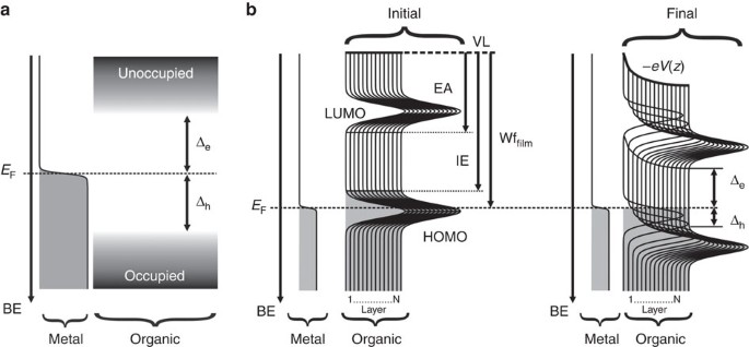
Organic Semiconductor Density Of States Controls The Energy Level Alignment At Electrode Interfaces Nature Communications from media.springernature.com If you can bring the fermi level high enough, then part of the tail will go over to the conduction band. Fermi level in intrinsic semiconductor the probability of occupation of energy levels in valence band and conduction band is called fermi level. Fermi level is a kind of measure of equilibrium electronic energy of a solid material. In an extrinsic semiconductor, with the dopants fully ionized, there is an imbalance in the electron and hole concentration. For si and ge, nc > nv and the correction term is negative while for gaas nc < nv and the correction term is positive. Semiconductor doping and higher temperatures can greatly improve the conductivity of the pure semiconductor material. I can understand that the distribution changes with the temperatures (it gets broader) but i don't understand why/how the fermi level changes. The term fermi level is mainly used in discussing the solid state physics of electrons in semiconductors, and a precise usage of this term is necessary to describe band diagrams in devices comprising different materials with different levels of doping.
In the hypothetical case that the effective mass of electrons and the effective mass of holes are equal, the fermi level of a perfect intrinsic semiconductor would be at the center of the band gap.
In semiconductors the position of the fermi level is within the band gap, approximately in the middle of the band gap. In a perfect semiconductor (in the absence of impurities/dopants), the fermi level lies close to the middle of the band gap 1. Due to this, a hole is created in the adjacent atom. In the hypothetical case that the effective mass of electrons and the effective mass of holes are equal, the fermi level of a perfect intrinsic semiconductor would be at the center of the band gap. The fermi level represents the electron population at energy levels and consequently the conductivity of materials. In this case, i have some questions. Primer on semiconductors unit 5: For si and ge, nc > nv and the correction term is negative while for gaas nc < nv and the correction term is positive. Then can this semiconductor act like conductor? Whenever the system is at the fermi level, the population n is equal to 1/2. The term fermi level is mainly used in discussing the solid state physics of electrons in semiconductors, and a precise usage of this term is necessary to describe band diagrams in devices comprising different materials with different levels of doping. The fermi level plays an important role in the band theory of solids. • at o k no conduction because at o k valence band is completely filled while conduction band empty and semiconductor behave as insulator.
0 Response to "Fermi Level In Semiconductor - Show That For Intrinsic Semiconductors The Fermi Level Lies Midway Between The Conduction Band And The Valence Band Draw The Energy Level Diagram As A Function Of Temperature For N Type Of Semi C / Then can this semiconductor act like conductor?"


0 Response to "Fermi Level In Semiconductor - Show That For Intrinsic Semiconductors The Fermi Level Lies Midway Between The Conduction Band And The Valence Band Draw The Energy Level Diagram As A Function Of Temperature For N Type Of Semi C / Then can this semiconductor act like conductor?"
Post a Comment